

Announced 26 Oct 2026 · Sources checked
What changed on NVIDIA's pages
NVIDIA has lowered several headline specifications for its Vera Rubin systems without an announcement. The Vera Rubin NVL72 product page, read by AI Lookout on 26 October 2026, lists each Rubin GPU with 288 GB of HBM4 memory and 19.2 terabytes per second of memory bandwidth. A Vera Rubin superchip, which pairs two Rubin GPUs with one Vera CPU, is listed at 576 GB and 38.5 TB/s. The full NVL72 rack, with 72 GPUs and 36 CPUs, is listed at 20.7 TB of HBM4 and 1,400 TB/s.
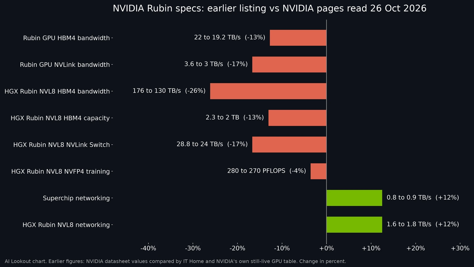
Those are not the numbers NVIDIA used before. IT Home reported on 26 October that it had compared NVIDIA's current documents with a copy of an NVIDIA document from June saved by a third party. In the June version, the superchip's GPU memory bandwidth was 44 TB/s, which works out to 22 TB/s per GPU. NVIDIA's earlier Vera Rubin datasheet listed the NVL72 rack at about 1,580 TB/s. Memory capacity per GPU is unchanged at 288 GB; it is the speed that came down, by roughly 13 percent.
NVLink, the connection that lets the GPUs in a rack share work as if they were one large chip, was cut by a similar share. The live page lists 3 TB/s per GPU, 6 TB/s per superchip and 216 TB/s for the rack. IT Home says the superchip figure used to be 7.2 TB/s, and the earlier rack figure was 260 TB/s, so the reduction is about 17 percent at every level. The compute figures on the page, such as 50 PFLOPS of sparse NVFP4 inference per GPU, were not part of the changes IT Home described.
There is also a small wording change for the CPU. Every Vera CPU used to be listed with 1.5 TB of LPDDR5X memory. The current pages say up to 1.5 TB, and up to 54 TB for a full rack, which leaves room for systems that ship with less.
The HGX Rubin NVL8 numbers
The cuts are larger on NVIDIA's eight-GPU server board. NVIDIA's HGX page now lists the HGX Rubin NVL8 and HGX Vera Rubin NVL8 with 2 TB of HBM4 and 130 TB/s of memory bandwidth across the eight GPUs. According to IT Home's comparison, the same systems were previously listed with 2.3 TB and 176 TB/s. That is about 13 percent less memory and 26 percent less bandwidth, which implies that the eight GPUs on this board now have less memory each than the 288 GB NVIDIA still quotes for a single Rubin GPU.
The NVLink Switch bandwidth for the board fell from 28.8 TB/s to 24 TB/s. Training throughput was also trimmed: the page now lists 270 PFLOPS of dense NVFP4 training and 130 PFLOPS of FP8 training, against 280 and 140 PFLOPS in the earlier listing. Inference throughput is listed at 400 PFLOPS of sparse NVFP4.
The HGX page is not internally consistent. Below the system table, a section of individual GPU specifications still lists each Rubin GPU with 288 GB of HBM4 at 22 TB/s and NVLink at 3.6 TB/s, the older figures. The marketing text on the same page has been updated to the new numbers and now says the board offers 2.1 times the memory bandwidth of an HGX B200, at 130 TB/s, and 1.7 times the NVLink Switch bandwidth, at 24 TB/s.
What went up instead
One set of figures moved the other way. Networking bandwidth, the speed of the connections that link one server or rack to others in a data center, went up. The NVL72 page lists 0.9 TB/s per superchip, 0.45 TB/s per GPU and 32.4 TB/s for the rack. IT Home says the superchip figure was 0.8 TB/s before, so the rack total would have been 28.8 TB/s. On the HGX boards, bidirectional networking rose from 1.6 TB/s to 1.8 TB/s.
IT Home also reports a much larger jump for the smaller Vera Rubin NVL4 configuration, from 0.4 TB/s to 1 TB/s of scale-out networking. That increase is larger than anywhere else in the lineup, and NVIDIA has given no explanation for it either.
Why memory bandwidth matters
For large language models, memory bandwidth is often the number that matters most. When a model writes an answer, each new token requires reading the model weights and the stored context from memory. On a fast accelerator that step is usually limited by how quickly data can come out of HBM, not by how many calculations the chip can do. A 13 percent cut in bandwidth per GPU can therefore mean a similar cut in the token rate of a memory-bound workload, even though the compute numbers NVIDIA quotes for inference stayed the same.
NVLink matters for a related reason. The largest models are split across many GPUs, and the parts have to exchange results constantly. A rack with 216 TB/s instead of 260 TB/s of NVLink bandwidth has less headroom for that traffic. Rubin is still a large step up from Blackwell on paper, which is how NVIDIA frames it on the HGX page. But the gap between Rubin and the previous generation is smaller than the figures NVIDIA had been publishing until recently.
The change also makes earlier performance claims harder to compare. Cloud providers and server makers have been quoting Rubin figures in their own launches, including Google Cloud's A5X instances built on Vera Rubin NVL72 and NVIDIA's own DSX POD containerized Rubin systems. Anyone who modelled capacity or cost per token on 22 TB/s per GPU now has a lower official number to work with.
Why the numbers might have moved
NVIDIA has not said why the specifications changed, and AI Lookout found no NVIDIA statement, blog post or footnote that mentions the revision. The pages carry no change log. The most common explanation in coverage of the change is about memory supply rather than chip design.
IT Home's reading is that a lower bandwidth target lets more HBM4 memory stacks meet NVIDIA's requirements and so raises the number of usable parts. Bandwidth in HBM depends on how fast each data pin can run, and memory makers have reportedly struggled to make enough HBM4 that runs at the speeds NVIDIA wanted. That is a plausible explanation, but it is IT Home's interpretation, not something NVIDIA has confirmed. NVIDIA is also pushing memory suppliers on a custom NVHBM design with base dies built on TSMC's 3nm process, which suggests it sees memory as a limit worth engineering around.
The timing fits a product moving from launch figures to shipping figures. The HGX page carries a banner saying Vera Rubin is ramping into full production, with Taiwanese server makers manufacturing and shipping systems. Final specifications are often set when a product reaches volume, and the chip industry has a long history of trimming clocks or memory speeds to match what can be built reliably in quantity. Even so, a silent edit to numbers that customers have already seen is unusual for a part this important.
What it means for buyers
For companies buying Rubin hardware, the practical question is which figure ends up in their contracts and acceptance tests. Purchase agreements for systems of this size usually reference a specific datasheet, and the systems are built by partners using NVIDIA's open MGX rack designs and parts, so the same GPU can reach a data center through several suppliers. Buyers who signed against older figures will want to know whether their systems are covered by those or by the new ones.
The rise in networking bandwidth may partly offset the change for some workloads. Training runs that span many racks spend much of their time moving data between servers, and faster scale-out links help there. Inference on a single rack gains less from that, because it depends more on memory and NVLink. The overall effect will depend on the model, the batch size and how the work is split, and it will only become clear once independent benchmarks of shipping Rubin systems appear.
What is still unknown
Several basic questions are open. NVIDIA has not said whether every Rubin GPU now ships at 19.2 TB/s, or whether some parts or later batches will run at the original 22 TB/s. It has not said whether the NVLink reduction comes from the GPUs, the switches or the cables, or whether the changes will carry over to Rubin Ultra and the products after it. The leftover 22 TB/s figure in the HGX page's GPU table could be an oversight, or a sign that the per-GPU specification is still under review.
AI Lookout did not contact NVIDIA for this article and relied on NVIDIA's public pages and IT Home's comparison. Until NVIDIA explains the revision, the safest assumption is that the current pages describe what customers will receive: Rubin GPUs with the same memory capacity as announced, about 13 percent less memory bandwidth, about 17 percent less NVLink bandwidth and somewhat faster networking.
Common questions
What is the memory bandwidth of the NVIDIA Rubin GPU now?
NVIDIA's Vera Rubin NVL72 page lists 288 GB of HBM4 at 19.2 TB/s per Rubin GPU, 38.5 TB/s per superchip and 1,400 TB/s per NVL72 rack. Earlier NVIDIA material used 22 TB/s per GPU.
Why did NVIDIA lower the Vera Rubin specs?
NVIDIA has not said. IT Home suggests a lower bandwidth target lets more HBM4 memory qualify and improves yield, but that is an interpretation, not an NVIDIA statement.
Did any Vera Rubin specs go up?
Yes. Networking bandwidth rose to 0.9 TB/s per superchip and 32.4 TB/s per NVL72 rack, and the HGX Rubin NVL8 boards went from 1.6 to 1.8 TB/s.
Sources & further reading
How this story was made
Written by Kristian Kostov with AI assistance and checked against the linked sources. Company performance claims are attributed to the company. Analysis reflects AiLookout’s interpretation; we have not independently tested the products discussed. The cover places the companies’ own logos, taken from public-domain or openly licensed files credited in the caption, on a plain background. It is not a product photograph, a screenshot, or an endorsement.
Our editorial standards