

Sources checked
Google expands its TPU portfolio to four systems
Google announced two new tensor processing unit systems on November 10, bringing its eighth-generation TPU lineup to four distinct chips released in a single calendar year.
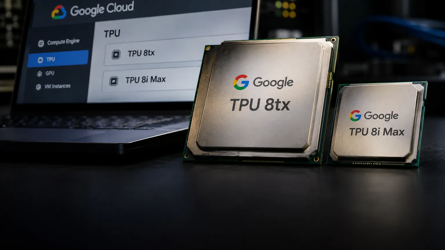
The new additions are TPU 8tx, a confidential inference chip co-designed with AMD, and TPU 8i Max, a dual-die system for massive context windows.
The company said the expansion addresses the shift from human-scale to agent-scale computing, where dozens of AI agents work together across entire codebases or hours of video simultaneously.
TechCrunch reported the launch comes as hyperscalers including Microsoft, Amazon, and AI labs like OpenAI and Anthropic build their own semiconductors to reduce reliance on Nvidia, whose dominant market position is facing its most serious competitive challenge in years.
The eighth-generation TPU family debuted in April 2026 with two systems: TPU 8t for large-scale training and TPU 8i for low-latency reasoning.
Google said at the time that TPU 8t and 8i offered up to 2.7 times better training performance and 80 percent better inference price performance versus the previous generation.
The two new additions bring the portfolio to four systems covering every stage of the AI lifecycle, from foundation model training to secure inference and long-context agentic workloads, putting Google in a position to compete with Nvidia across the entire AI hardware stack.
TPU 8tx brings hardware-level security to confidential AI
TPU 8tx is built on the same silicon as the training-focused TPU 8t and paired with 5th Generation AMD EPYC CPU hosts.
Google said the chip "builds security directly into the hardware layer, keeping sensitive data and model weights protected and isolated even while in active use."
Normally, data is encrypted at rest and in transit but must be decrypted in memory during processing, creating an exposure window.
TPU 8tx closes that gap with hardware-level confidential compute, making it suitable for regulated enterprises and governments running frontier or proprietary models.
The AMD EPYC integration is significant: AMD's SEV-SNP technology encrypts VM memory at the hardware level, and Google has extended that protection into the TPU interconnect itself.
The chip also includes a custom inferencing network that lets it run reasoning alongside training, so organizations can fine-tune models using private data, distill large models into smaller ones, and serve them on a single system all without moving data between devices.
Google described TPU 8tx as "built for the agentic era," where autonomous agents execute sensitive enterprise workflows like analyzing financial records, processing medical data, or auditing internal systems without exposing the data at any point in the pipeline.
The confidential inference market is growing fast as enterprises adopt proprietary models trained on internal data. Nvidia recently launched its own confidential bare-metal GPU instances, and the major cloud providers are racing to offer hardware-level isolation for AI workloads.
Google's TPU 8tx differentiates by integrating security at the system level rather than as a software overlay, which reduces the performance overhead that typically comes with encryption for confidential computing scenarios.
TPU 8i Max tackles the memory wall for agent workloads
TPU 8i Max combines two low-latency TPU 8i chips on a single package, delivering double the compute, double the SRAM, and double the HBM bandwidth of a single TPU 8i.
Google said the system prevents large workloads from stalling by keeping processors equipped with essential data, a design choice that directly targets the memory wall problem that has become the defining bottleneck for long-context inference workloads.
The memory wall has become the defining bottleneck for frontier AI workloads.
As models grow to millions of tokens of context, the KV cache alone can exceed available HBM on a single chip, forcing systems to spill to slower memory tiers and degrading latency.
TPU 8i Max addresses this by doubling the on-chip SRAM and HBM capacity, letting larger portions of the context stay close to the compute units for faster generation.
Google also open-sourced TPU Sync, a model-state layer that turns chip HBM, host DRAM, shared storage, and the data center network into a single memory hierarchy.
It automatically tiers massive KV caches off the chip in milliseconds, bringing data back to HBM only when needed for the next inference step.
This approach mirrors the virtual memory concept in operating systems but is optimized for the sequential access patterns of autoregressive generation.
The company said its native vLLM-TorchTPU software stack on TPUs achieved state-of-the-art price-performance marks on MLPerf-style benchmarks for agentic coding and long-context workloads.
The stack combines the throughput of vLLM with TorchTPU's optimized kernel compilation, allowing teams to run production inference without writing custom CUDA kernels.
Open software stack targets every PyTorch developer
Alongside the hardware, Google made several software announcements aimed at lowering the barrier to TPU development. PyTorch code and Hugging Face models now run natively on TPUs, and the company released out-of-the-box backends for open-source inference engines vLLM and SGLang.
This means any team already using these popular frameworks can target TPUs without rewriting their pipelines.
Google also introduced TPU Guru, an AI agent now in preview that plugs into coding tools like Claude Code, Cursor, and Google Antigravity to automate TPU onboarding, diagnose bottlenecks, and autotune custom kernels using plain language.
For production, a new open-source C++ runtime lets teams train models in Python and serve them directly across TPUs, GPUs, and CPUs, abstracting away the hardware differences.
The broader industry context matters. Nvidia remains the dominant AI chip supplier, but its CEO Jensen Huang is facing a spy scandal and shareholder lawsuit, creating an opening for competitors.
With these additions, Google's four-system eighth-generation TPU lineup now covers every stage of the AI lifecycle: TPU 8t for large-scale training, TPU 8i for low-latency reasoning, TPU 8tx for secure confidential inference, and TPU 8i Max for massive context windows.
Google has also signed deals with Oracle to bring TPUs to Oracle Cloud Infrastructure and with OpenAI to supply TPU chips, signaling that it sees the TPU business not just as an internal accelerator but as a commercial product competing directly with Nvidia in the cloud AI chip market.
Common questions
What is TPU 8tx?
TPU 8tx is Google's confidential inference chip, built on TPU 8t silicon with 5th Gen AMD EPYC hosts. It provides hardware-level security for sensitive data and model weights during processing, targeting regulated enterprises and governments running proprietary models.
What is TPU 8i Max?
TPU 8i Max combines two TPU 8i chips on a single package, doubling compute, SRAM, and HBM bandwidth.
It is designed for massive context windows and agentic workloads where dozens of AI agents work together across large codebases or hours of video.
When are the new TPUs available?
Google announced both TPU 8tx and TPU 8i Max on November 10, 2026. Pricing and general availability dates were not disclosed in the announcement.
Sources & further reading
How this story was made
Written by Kristian Kostov with AI assistance and checked against the linked sources. Company performance claims are attributed to the company. Analysis reflects AiLookout’s interpretation; we have not independently tested the products discussed. The cover is an AI-generated editorial illustration, not a photograph or evidence of an actual event.
Our editorial standards